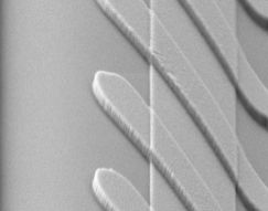
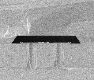
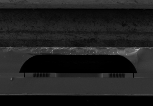
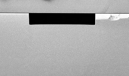
With our complete MEMS advanced process modules as building blocks, multiple process platforms have been built for the fabrication of MEMS devices on Si, Glass, SOI and cavity SOI substrates. These process platforms expedite the fabrication iterations for customer's design validation and the product time-to-market. APM continues on deepening and widening its platform categories, and smooth the integration between them. Meanwhile, we tailor process flows in order to meet customer's special requirements.
Substrate Technology
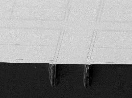
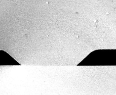
Cavity SOI / Layer Transfer Technology
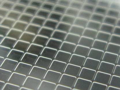
SOG (Silicon on Glass) / Structured Glass and Glass Wafer Process

.jpg)