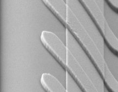
The abundant MEMS advanced process modules (also known as building blocks) form the foundation of our wafer processing service and can be utilized on Si, Glass, SOI, and Cavity SOI substrates. These process modules expedite fabrication iterations for customer design validation and shorten the product time-to-market. APM continues to deepen and expand its process module categories and streamline their integration to meet customers' specific requirements.
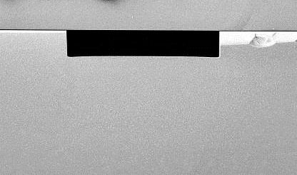
Substrate Technology
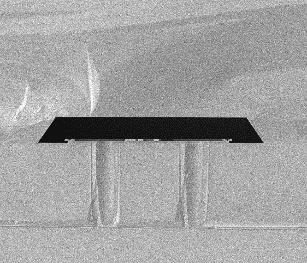
Cavity SOI / Layer Transfer Technology
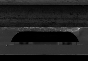
SOG (Silicon on Glass) / Structured Glass and Glass Wafer Process

.jpg)